Why PCB Designing?
We often come across two scenarios where we need PCB designing. Sometimes we need to fix a medium/large sized circuit with various components into a smaller and more compact form. And sometimes we need to use a specific circuit more number of times. In such cases, making a Printed Circuit Board of the required circuit is very useful.
Have a look:
What is Eagle?
Eagle is a PCB Designing Software where you can use custom libraries for using a variety of elements, from common Resistors, Capacitors etc to specific ICs, Microcontrollers. It lets you add the elements you want, design the circuit and the choose the physical connections the way you want on your PCB.
Details Of Commands and usages in making the SCHEMATIC
There are basically two parts of our development in Eagle. First, the Schematic, that shows all the connections(but not the way you physically want on the PCB). Secondly, forming final connections and arranging them in the final physical way we want.
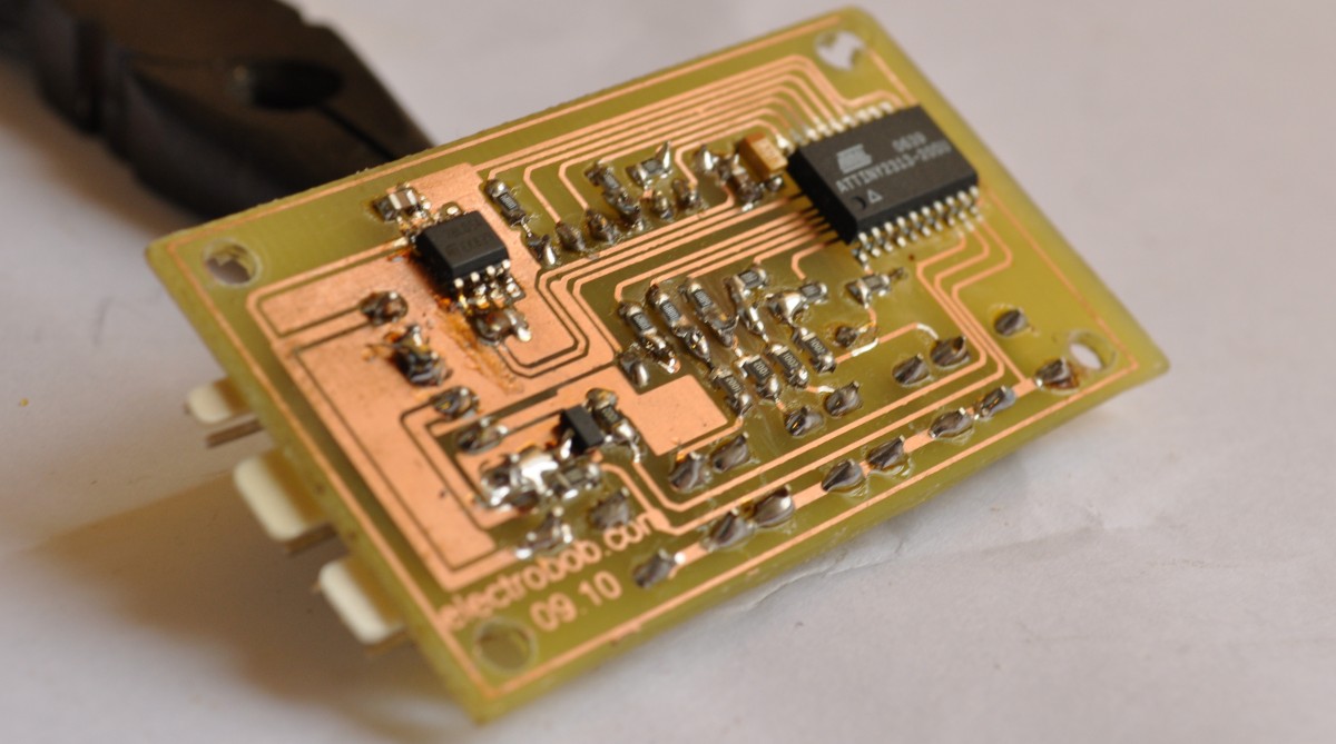
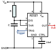
So, in the session, we decided to make a IC 555 circuit.
We will go through the following procedure:
-
Making the Schematic
-
Designing the physical connections
Let us move on to using the software and its commands.
1. Making the Schematic
- add: Used to add any component. Type in the command bar on top
- After performing add, lots of components will appear. Type keywords to search components. Eg. RCL in search box to find Resistor, Capacitor, Inductor.(Take US Package for resistor.) (uF == Polarised, nF == ceramic)
- For NE555N type:add on terminal> search timer > Find 555. Double click>Paste.
- Note:- Whenever IC not found, Google the .lbr file for that IC and copy paste in Eagle list.
- Use Escape to go back to menu.
- For our 555 circuit, we will take a 5mm LED for Output
- Type Supply in search bar to get 5V and Ground
- move: to move a component
- net: make connections. Net adds connection and side by side makes a file(which denotes that there must be a physical connection made for this pair in the second part of our designing) too.
- Make end to end connections and use name command to name the wires/components differently so as to differentiate between connections.
- Giving values: Use value command and then click on component to enter value.
- Smash command: to move around names.(Disassemble components to move individually)
- Search Pin Head for Berg Pins!
- Right click a component to rotate
- Delete command and select the “plus” sign (appearing at centre of component on zooming) denoting the component to delete it.
- Label command to show the labels.
You are expected to be done with the schematic using these commands.
Now Type Board command and click Yes option to go to the next part.
2. Making the Physical Connections
- Air Line: denotes a connection that must be made(shows that these two points ought to be physically connected).
- Tools>Ratnest:Simplifies air wire connections(because the connections change with the physical positions of components and so, they can also overlap)
- Change package: helps to change the type of component.
- Note: - If you made wrong connections and want to change a component, do it in the schematic file (part 1) and not here.
- Menu>Autorouter is used to find the possible physical routing by eagle’s own algorithm. It will return certain best possibilities, based on certain criteria.(Note:- Menu>Autorouter>Uncheck Continuous Option while auto routing again). In case of Single Layer PCBs(we mostly have only single layered ones):Top is Not Applicable.
- We can do manual routing by Route Command.
- Width of the connection is given in Inches, around 0.024 inches is a preferred width(it shouldn’t be very small because not many printing facilities may have that accuracy).
- Change track shape by Right click(Avoid using right angles because of some
- Ripoff command changes a physical connection back to just an air wire.
- It might be useful to create a common ground/power line around the PCB, it sometimes simplifies the complexity of connections.
- Make sure to Save the file in the same folder as the project.
To make final output files for Gerbv:
- File > Cam Processor.
- File > Open > Job == gerb274x.cam
- Process Job In bottom
To see the final files in Gerbv:
- Open the files with following extensions
.brd, .cmp, .plc, .sol, .stc, .sts. - Using the text command, you can write text anywhere. Use it for specifying stuff to make circuit connection and component placement easier. Add these names for reference by choosing layer tNames and adding text.
- Change board size using move command and moving the boundaries.