ATMEL’s AVR Series of Microcontrollers is a very good option for those who wish to use the microcontrollers to their true potential, exploiting every bit of functionality they can offer. Learning them requires you to sometimes indulge into the internal aspects of microcontrollers. Registers, Binary Numbers all play a major role in operating these microcontrollers in their hardcore form. They form the heart of the Arduino Microcontrollers you might have learned earlier.
The AVR Series has many microcontrollers which vary in their processing capacity(Speed) and Memory. Throughout this tutorial we shall consider ATMega16 as our sample.
(ATMega32: 8-bit AVR Processor, 16 kbytes flash memory)
Contents:
Installation
In order to write the code for AVR, and to burn it to the microcontroller, we use the software provided by ATMEL: ATMEL Studio.
We also need something that connects the microcontroller and the computer (by USB). This was very simple in case of Arduino because among its peripherals, there was an in-built USB slot. Here we will use a “Development Board”.
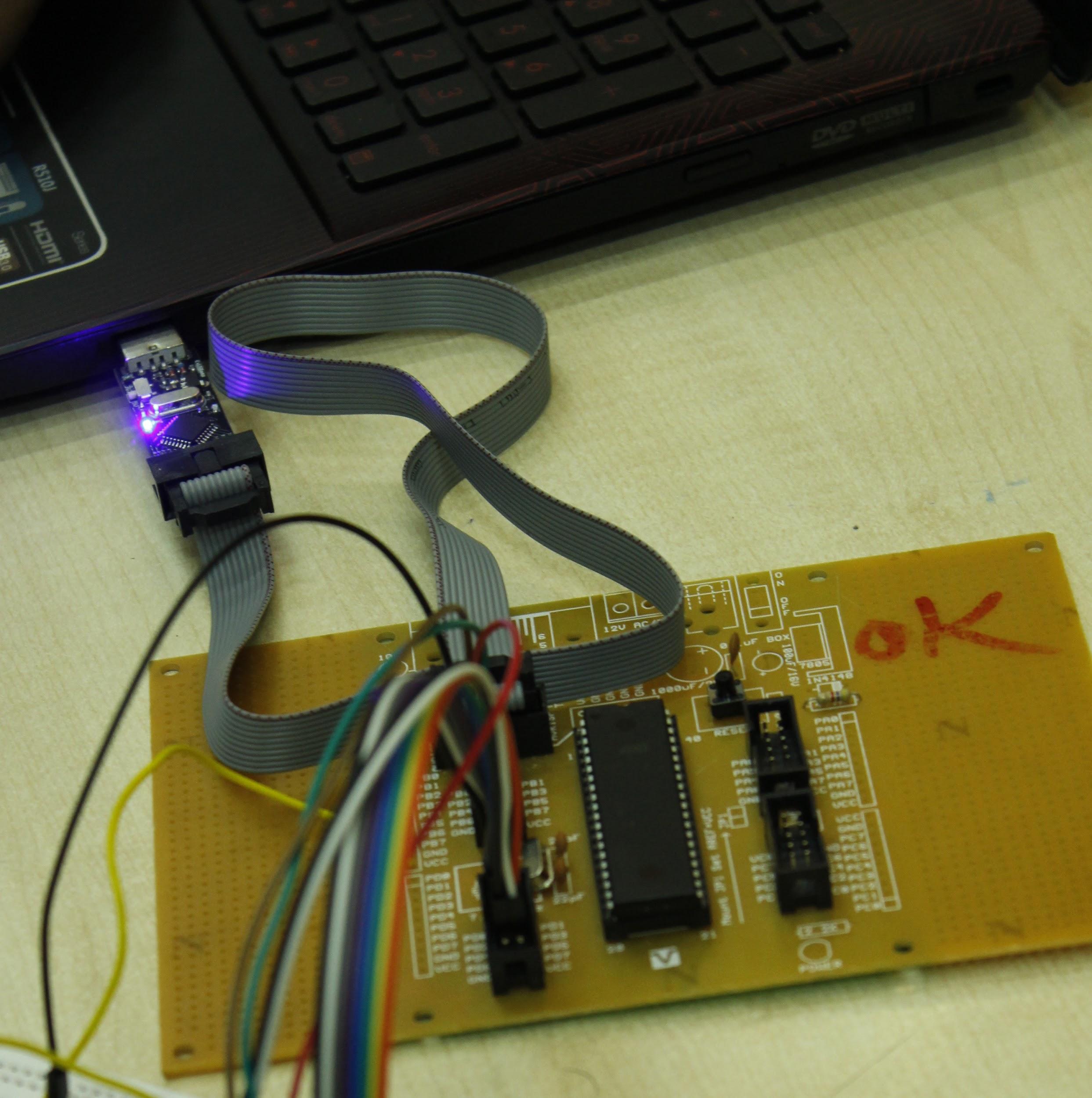
In the picture above, observe 2 main things:
- The Programmer, which is plugged in the computer USB slot: It is used for the development board-to-USB Slot interface.
- The Development Board: Provides an interface to connect pins with Jumpers to further circuitry and with the input of the programmer.
After this let us move on to installation of ATMEL Studio.
Download Atmel Studio
Get the software setup here: http://www.atmel.com/tools/ATMELSTUDIO.aspx.
Install Drivers
After installing Atmel Studio 7, we need to install Drivers for the programmer. Refer to the following videos for the procedure.
For setting up avrdude: Microcontroller Programming Environment WinAVR Install
And for configuring the USBasp tool: Microcontroller Installing Atmel Studio
Atmel Studio has the environment for writing and compiling the code for AVR Microcontrollers, but in order to program the microcontroller with a programmer (the chip with an LED at the USB slot in the above picture), we need to configure the software with a new tool. For this configuration, we must set up avrdude (Video 1).
Now, for configuring the USBasp tool we need to set certain things since it is different than the normal USBs which we use at the ports. For this we need to configure the new external programming tool as specified in Video 2.
These two steps are very important and it will not be possible to write the code to the AVR Microcontroller properly without getting these configurations right. Refer the given links properly and if you have any doubts you can ask on the Electronics Club Gitter Rooms.
Installation for Linux
You need to install three packages, gcc-avr,avr-libc and avrdude for compiling and burning to AVR microcontrollers
On ubuntu you can run the command
sudo apt-get install gcc-avr avr-libc avrdude
After that we have prepared a Makefile to compile and burn AVR code on linux. You can download the Makefile here.
Copy this Makefile into your project folder and open it in a text editor. You
need to edit the first line of the file to be PROJECT = <filename>. For eg.
if the name of your main C file is test.c, your first line should be
PROJECT = test
Then run
make
to compile the code and generate HEX file. Then run
sudo make burn
to burn HEX file to AVR after connecting USBasp.
Basics of AVR
Pins
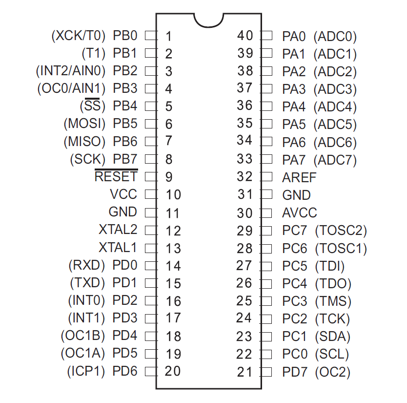
Confronting the Pin Diagram of ATMega16 at this stage can be a little dangerous for your enthusiasm, so please proceed slowly.
Apart from the Power pins, all the pins on AVR can be configured as Input or Output. These pins are present in four groups, or “Ports”, namely PortA, PortB, PortC, PortD. Every pin is given a name, like PA0,PB5 etc associated with its port. Besides every pin, its special function is mentioned in brackets. For example, all pins of PORTA can be used for ADC purpose apart from regular digital input/output. In this way each pin has a special function. So, we have 8x4=32 normal I/O pins, and 8 different pins meant for power supply, ADC voltage reference, reset etc.
Pinout for ATmega16
Registers
The microcontrollers(uC) use Registers to store the data describing the state(or mode) of certain operations(in most of our cases). For example, there is a register to store the “state/mode” of pins in every port, whether they are input or output pins. The Timer/Counter Control Registers(TCCR1A/B) store information regarding timers and counters(certain parameters etc). Similarly, there are many registers and they store bytes that control most of the functions of the microcontroller, so, the High/Low states of bits of those registers enable/disable interrupts, ADC etc.
The first register we will see is the one I just described. It is called the Data Direction Register(DDR). Hence DDRA is the register(8-bits of data) showing Input/output states of the 8 pins in port A.
Using the Datasheet
Though very intimidating to look at, the datasheet can provide you with just the right information if you know how to use it, and if you know that you have to use ‘IT’.
It is not at all necessary to read the complete datasheet, but there are portions in it which are at our level of understanding and there is also useful information which we will certainly need on our way.
It contains the code for every register, i.e. which bit of the register stores data for what function and lot of other information which we will use.
So keep the datasheet handy!
Get it here: http://www.atmel.com/devices/atmega32.aspx?tab=overview.
Controlling Input and Output
As stated earlier, one of the registers called Data Direction Register is used to control whether the pin acts as an Input pin or an Output pin.
Thus we have four 8-bit registers:
DDRA/B/C/D for controlling 8 pins each, of Ports A/B/C/D.
The convention for setting the input/output bit is:
1 - Output pin i.e. Controlled by Microcontroller
0 - Input pin i.e. Controlled by external circuit
Controlling the Output
Now, for the Output Pins, in order to set them to the value we wish, we use another register PORTA/B/C/D. Thus PORTA is a 8-bit register, which stores the 8 bits corresponding to each pin of Port A(effectively only the Output pins) for whether to give it a HIGH or LOW state.
Let us convey all this through a code snippet.
DDRA = 0b00001101;

PORTA = 0b00000101;
Note: The order of pins is 76543210, i.e. Most Significant Bit corresponds to pin 7
This tells the microcontroller that:
- Line 1: Pins 0,2,3 of Port A should be declared as output pins and rest as input.
- Line 2: Pins 0,2 should should give HIGH(Vin) and 3 should give LOW(0) output.
The bits corresponding to input pins of present in PORTA don’t matter, that is PORTA is an Output only Register
Reading the input
For the input values, there is a similar Input only Register, PINA/B/C/D.
The values of inputs are stored onto this 8-bit register, and in the code, we use this register with the comparison operator.
This statement:
PINA == 0b11000010;Checks if the inputs on pins 7,6,5,4 and 1 are High,High,Low,Low and High respectively.
Bitwise Operations
Bit masking refers to accessing specific bits in a data and modifying them according to our needs. Bit operations are a way to implement masking.
Bitwise Operators available in C are: AND (&), OR (|), XOR (^) and NOT
(~). There are also bit shift operators viz. Bit left shift (<<)
and Bit right shift (>>) operators.
Bitwise operators are the ones that are defined on 2 bits and hold for large binary number through bit-by-bit binary operations and defined on 2 bits.
Boolean Algebra
AND (&)
Works like regular logical AND(A.B). So, for PORTA = 0b01101111 = 0x6f and PORTB = 0b10011001 = 0x99,
PORTA & PORTB = 01101111 & 10011001 = 00001001 = 0x09.
OR(|), XOR(^), NOT(~) work in the same way. They are same as their
logical functions for 2 bit operations, and for larger numbers(many
bits) they are executed bit by bit using binary model for each bit
pair(as shown in bitwise AND example).
Bit Shifting
As the name suggests these operation are used to shift the position of a
bit by some particular places. If you use << then the bits are
shifted to the left, and if you use >> then the bits are shifted
to the right and the bits are shifted by the number of places return
besides these symbols.
Binary Left Shift Operator
This shifts left operand value to left by number of bits specified in the right operand. In other words, Binary left shift moves bits to a specified number of places to the left. The least significant bit is appended with 0 and most significant bit is dropped. The value of the variable gets multiplied by 2 for every left shift that occurs.
If PORTA=01101111,
Then PORTA << 3 = 01111000;
Binary Right Shift Operator
This shifts left operand value to right by number of bits specified by the right operand. The most significant bit is appended with 0 and least significant bit is dropped.The value of the variable gets divided by 2 for every right shift that occurs.
PORTA >> 2 = 00011011;
Usage in AVR
Bit Operations are used very often, wherever the logical operations are required.
Bit Shifting is very useful in setting only specific bits of registers without worrying about everything else on the register.
If you wanted to turn on the lowest bit on PORTA, then you can simply write a 1 to PORTA because a 1, in 8 bit binary, is really 00000001.
PORT A = 1;
However, if you wanted to turn on the second lowest bit on PORTA, then an easy way to do it is with a bit shift:
PORTA = (0b00000001<<1);
Example:
PORTA = 10001001;
Means the same as
PORTA= (1<<7) | (1<<4)| (1<<0)
Bit Masking
Bits in registers are given names. We will discuss TCCR1B later here, but for the time being assume that a register has a bit named CS10. The usefulness comes out of the fact that you can set the CS10 bit High just by executing:
TCCR1B = (1<<CS10);
That is, “CS10” acts as its numeric location on the register! Bit Masking is used to carry out operations on only specific bits from a number of many bits.
Instead of TCCR1B = 1<<CS10 | 1<<CS11,
It is better to write: TCCR1B |= 1<<CS10 | 1<<CS11.
It lets the other bits stay as they are(OR with 0) and only sets the
selected bits high(from low).
Timers and Counters
The operations in any microcontroller are “sequential” at heart, and so they all rely on clock-pulses. Hence the microcontrollers have internal clocks that keep ticking at the given rate, irrespective of anything else happening around them. They can also use external clocks for this same purpose.
The timer and counter functions in the microcontroller simply count in
sync with the microcontroller clock. But the counter has limitations
due to its bit-capacity, i.e. a 8-bit counter can count only up to
256(or 0 to 255). So generally there is a 16-bit counter(65536 counts).
The counts are stored in the most important Timer/Counter Register,
TCNT1(16-bit, by default).
Pre-scaling
Now compare the maximum count of a counter and the clock-ticks of a microcontroller. Standard AVR Microcontrollers generally operate at 1 Mhz, that is 1,000,000 ticks per second, which is much more than 65536!
Hence, we need “prescaling” to increase the time-range of one cycle of the counter(they start all over again after attaining the max value) to a time comparable to our physical time domain(seconds). Prescaling is a way for the counter to skip some clock ticks.
AVR Microcontrollers allow prescaling of: 8, 64, 256 and 1024.
So, by setting a “Prescaler” of 8, the counter counts only once for
every 8 ticks of the microcontroller clock, i.e. it runs at F_CPU/8
(F_CPU = Frequency of uC).
Registers for controlling timers/counters
The register TCCR1A and TCCR1B (Timer/Counter Control Registers) are used
for this. Please refer the datasheet for the description of the
registers.
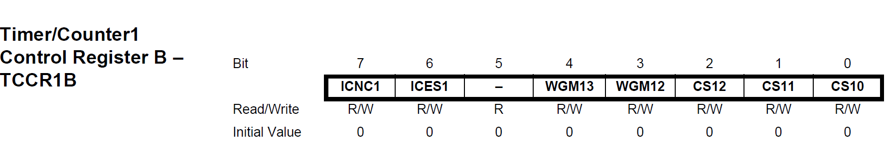
As you can see, all the 8-bits in the register are named.
(No need of knowing the function of all the 8 bits at this stage, the relevant ones will be discussed next)
Let us understand this through our first code on ATMEL Studio.
First code: LED Blink
Using the concepts learnt till now, we will write a program to toggle an LED 7 times a second.
We will proceed in a way in which you will have to, when you are doing it yourself. That is, we will use the Datasheet for reference instead of direct steps given to you.
How to choose the correct prescaler?
The uC ticks 1,000,000 times a second. We want to toggle the LED 7 times a second. So, we want the LED to toggle on every 142857th clock pulse. Now, since 65536 (highest value of count) is smaller than 142857, we want to set a prescaler such that “the highest count comes well after the time when the original uC clock reaches 142857” (Read this line twice :p). 8, 64 are suitable prescalers. Let us take 64.
Okay. I got the prescaler. Now how do I set that?
Search “prescaler” and after some experience you will know where to look, among the numerous results you get for “prescaler” :p.
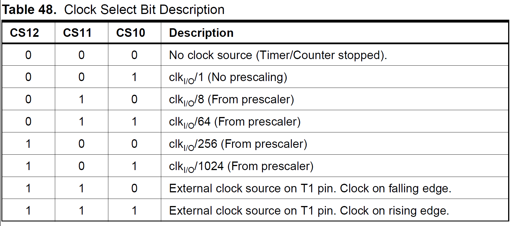
In the relevant table you will find the bit combination of CS12/11/10
required to set the prescaler we want. In our case: CS12/11/10=0/1/1
respectively. So we set the bits accordingly, using concepts of bit
shifting and bit masking as discussed earlier.
(I told you about TCCR1A/B earlier, but ideally you first discover
CS12/11/10 and then find out that these bits are present on TCCR1B,
going by the datasheet approach :p)
When to toggle the LED?
On every 142857th pulse of the uC clock. That is, when TCNT1 is at the
142857/64 = 2232th count (for prescaler=64).
After this background have a look at the actual code required for this.
Code
#include<avr/io.h>;
int main(){
DDRB = 0b00000001; //Pin B0 becomes output pin
PORTB = 0b00000000; //set B0 to Low
TCCR1B |= 1<<CS10 | 1<<CS11; //set Prescaler
while(1){
if(TCNT1>2232){ //2232=65536/7
TCNT1=0; //reset counter
PORTB ^= 1<<PINB0; //toggle LED
}
}
}Theory of Interrupts
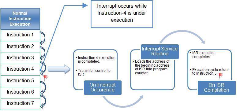
Interrupts are events that have the highest priority for the microcontroller(it pays immediate attention to them). That is, when an interrupt event occurs, the microcontroller Pauses its current task and attends to the interrupt. This is done by executing a routine called Interrupt Service Routine(ISR). At the end of the ISR, the microcontroller returns to the task it had paused and continues normally. So ISR or Interrupt Handler is the piece of code that must be executed when an interrupt is triggered.
Now, for enabling the execution of interrupts, we need to give appropriate values to certain bits, in certain specific registers. One compulsory bit is the Global Interrupt Enable bit. That is, when an interrupt flag is raised, the global interrupt bit must be High, in order to forward that interrupt request. So it is like an And-filter: “Request an interrupt if that specific interrupt flag is raised AND the global interrupt is enabled.”
A “flag” is like the abstract-physical representation of a bit for an event :p
Apart from the global interrupt enable bit, we have interrupt enabling bits for all the ways in which interrupts can be triggered. They can be triggered through the following ways:
- ADC
- Timer matching a given count
- Pin being High/Low
- Serial Communication
Timer triggered interrupt
Now let us apply our theory in writing a code for triggering an interrupt when the timer reaches a certain count.
We still need to know about the specific bits to be set for triggering an interrupt by comparison with timer. This is done by Clear Timer on Compare Mode.
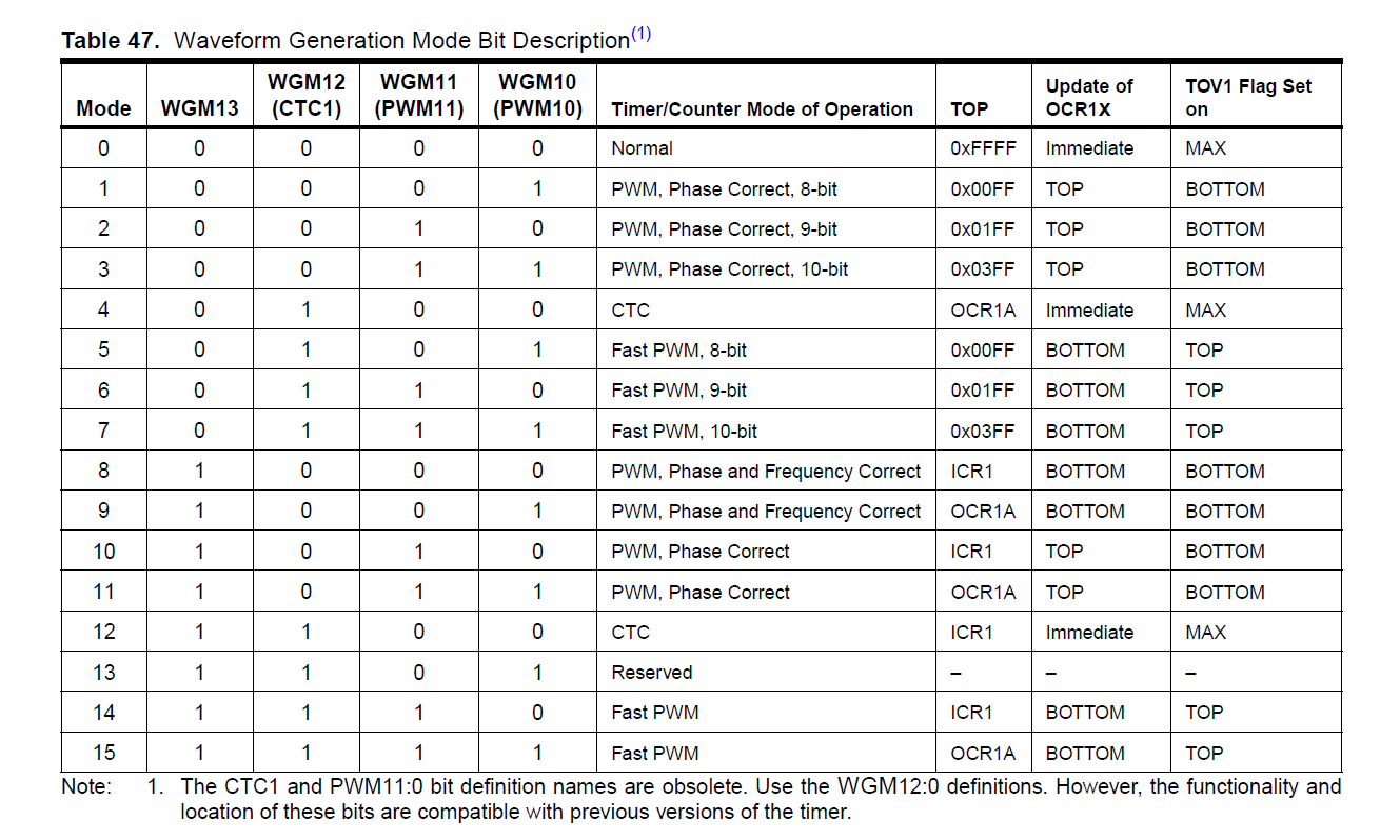
See option 4. This mode clears(resets) the timer on matching with a given value.
We also need to enable the time-match-triggered interrupt.
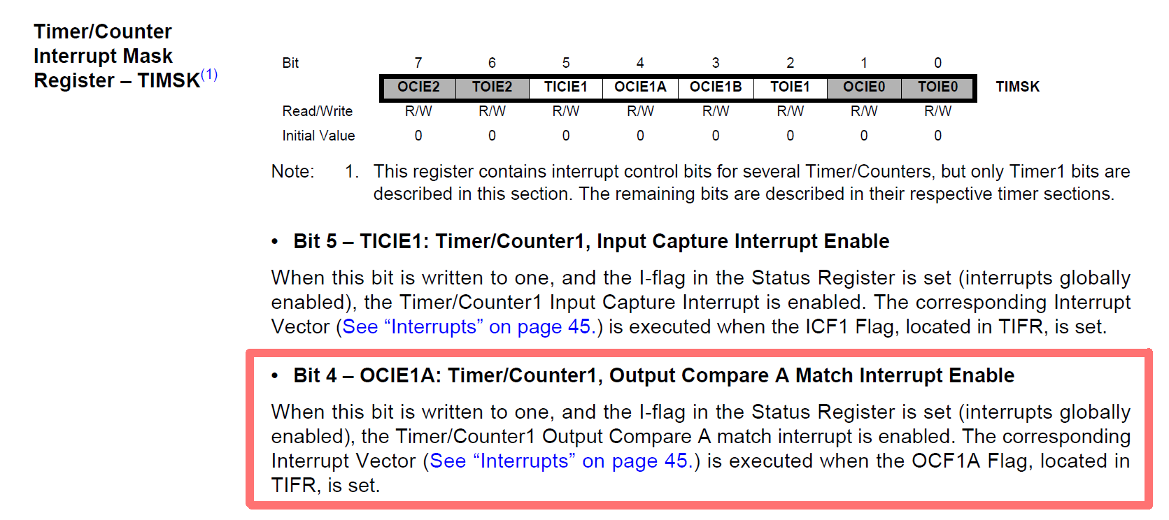
We will set OCIE1A bit High, thus enabling it. So, when the timer
reaches the value specified(stored) in OCR1A, timer will be
cleared (“Clear on Compare”) and the Output Compare Match Interrupt
Enable becomes high (Interrupt flag raised).
Once the and interrupt is requested(global interrupt must be enabled), uC will go into the ISR, so we will specify the code for the ISR also.
Code
#include<avr/io.h>

#include<avr/interrupt.h>


int main(){
    sei(); //enable global interrupt

    DDRB |= 1<<PINB0;
    TCCR1B |= 1<<CS10 | 1<<CS11 | 1<<WGM12; //set prescaler, and enable CTC

    TIMSK |= 1<<OCIE1A; //Timer1 Output Compare A Match interrupt enabled

    OCR1A = 15624; //Value at which CTC

    while(1){}
}

ISR(TIMER1_COMPA_vect){ //Checks argument

    PORTB ^= 1<<PINB0;
}
Analogue-Digital Conversion
Microcontrollers are capable of detecting binary signals i.e is the button pressed or not?.
It interprets five volts as 1 and zero volts as 0. The world however is not so simple and likes to use shades of gray. What if the signal is 2.72V? A 5V analog sensor may output 0.01V or 4.99V or anything inbetween. Microcontrollers have a device built into them that allows us to convert these voltages into values that we can use in a program to make a decision.
The ADC reports a ratiometric value. This means that if the ADC is a 10 bit ADC then it assumes 5V is 1023 and anything less than 5V will be a ratio between 5V and 1023. Hence we can see analog to digital conversions are dependant on the the reference voltage(which is by default the system voltage).
In microcontrollers we have the flexibility of setting the reference
analog voltage for the ADC.There’s a pin available on the
microcontroller called as AREF which can be set to desired values
and you can have your customized ADC. For example in a 10 bit ADC if the
input voltage is equal toAREFthen the ADC output is 1023. If the input
voltage is less thanAREFvoltage then the ADC output is somewhere
between 0 - 1023.
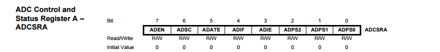
As you know, we need to set certain bits in some registers in order to use ADC.
- ADC Multiplexer Selection Register (
ADMUX): For selecting the reference voltage and the input channel. - ADC Control and Status Register A (
ADCSRA): As the name says it has the status of ADC and is also used for controlling it. - ADC Data Register (
ADCLandADCH): The final result of conversion is here.
Here’s the logic flow for algorithm for using ADC:
- Enable global interrupts
- Selecting the correct clock frequency for maximum resolution ( 50 – 200 KHz)
- Selecting the input pin
- Set the ADC Interrupt Enable
- Enabling the ADC
- Start the ADC conversion
The descriptions of these registers, and the relevant tables for deciding the bit combinations as given in the datasheet are shown below.
Based on the tables that follow, which bits are set to what value for achieving what setting is mentioned in the code comments.
ADSCRA
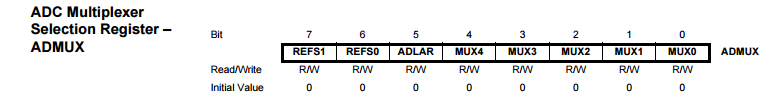
ADMUX
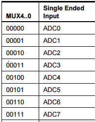
Selecting Input Pin
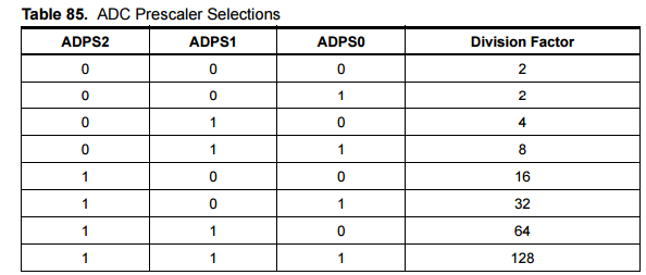
Setting ADC Prescaler
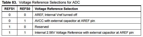
Reference Voltage Selection
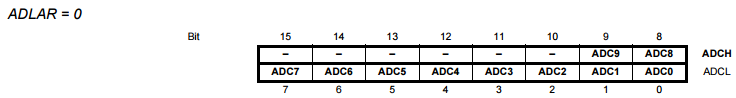
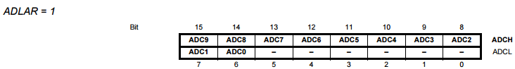
Registers for storing the digital output (available in two formats)
The result, which is a 10-bit number is stored here, and thus 8 bits
together and two bits after/before the 8
bits (ADLAR=0/1).
Code
For ADLAR=0
#include <avr/io.h>

#include <avr/interrupt.h>


int main(void)
{
    ADCSRA |= 1<<ADPS2; //ADC Prescaler = 16

    ADMUX |= (1<<REFS0) | (1<<REFS1); // Reference Voltage = 2.56V

    ADCSRA |= 1<<ADIE; // Enable ADC Interrupt

    ADCSRA |= 1<<ADEN; //Enable ADC

    sei();
    ADCSRA |= 1<<ADSC; //Start Conversion

    while (1){};
}

ISR(ADC_vect)
{
    uint8_t low_1 = ADCL; //a datatype of 8 bits, unsigned

    uint16_t output_ans = ADCH<<8 | low_1; //similar, but 16 bits, concatenated with upper two bits in ADLAR

    ADCSRA |= 1<<ADSC; //Start again

}
For ADLAR=1
#include <avr/io.h>

#include <avr/interrupt.h>


int main(void)
{
    ADCSRA |= 1<<ADPS2;
    ADMUX |= (1<<REFS0) | (1<<REFS1) | ( 1<< ADLAR ) ; //ADLAR=1 this time

    ADCSRA |= 1<<ADIE;
    ADCSRA |= 1<<ADEN;

    sei( );
    ADCSRA |= 1<<ADSC;

    while (1){}
}

ISR(ADC_vect)
{
    uint8_t low_1 = ADCL;
    uint16_t output_ans = ADCH<<2 | low_1>>6; //merging is slightly different

    ADCSRA |= 1<<ADSC;
}
Pulse Width Modulation
As you might know, PWM is a technique to produce Analog-looking output by digital means. We discussed the same in our Arduino Tutorial(LINK HERE), and you can refer the theory of PWM here: https://www.arduino.cc/en/Tutorial/PWM.
Its main use is to control the power supplied to inertial loads like motors. An average value of current/voltage is supplied to the load by turning the switch on off very fast, at a particular frequency.
While in arduino, we had the ready-made command analogWrite() for this,
here we will have to engineer the whole procedure :p.
We need to the following things in order to execute PWM in AVR:
- Know the PWM Enabled pins.
- Calculate the duty cycle, hence the time(within one cycle) when to turn the switch on/off.
- Set the correct bits(High/Low) for enabling PWM in the microcontroller.
Use the Datasheet to find various Modes in which we can use PWM(Waveform
Generator). We will use the Fast PWM Mode, with ICR1 as Top-most
value.

Another thing to be specified is here:
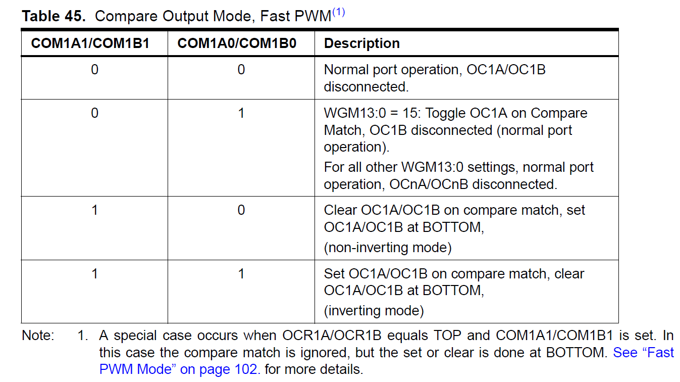
We will choose the 4th option, i.e. COM1A1 and COM1A0 High, so OCR1A is
cleared when it reaches our count from reverse(the top). Let us see this
through code:
Code:
#include <avr/io.h>


int main(void)}{

    DDRD |= 0xFF;
    TCCR1A |= 1<<WGM11 | 1<<COM1A1 | 1<<COM1A0;
    TCCR1B |= 1<<WGM13 | 1<<WGM12 | 1<<CS10;
    //These two lines enabled Fast PWM, set the inverting mode and gave a prescaler of 1 (no prescaling)


    ICR1A = 24999;
    // We assume the frequency we want, and divide it by F_CPU to get the count

    // In this case, we have set a frequency of 40 Hz


    OCR1A = ICR1A - t; // t is the time for which u want the pulse to be high

    // We are using the inverted mode, hence we assign from the end

    // t can be any value from 1 – 24998 :P


    while (1){}
}
Here, duty cycle of (t/24999)*100% will be achieved because, in the
inverting mode OC1A/B is cleared at bottom, and set(High) on match.
Interfacing with LCD
Anatomy of the LCD Screen
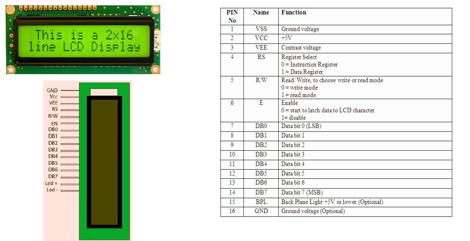
Controlling the LCD
There is an instruction set for the LCD, which specifics the specific
setting of bits RS, RW and DB0 to DB7, for giving specific commands to
the LCD. But that is the internal functioning, we do not need to indulge
into all of this. Instead, we have a header file wherein each
instruction(combination of bits High/Low) is mapped to a function in C.
So we will use this header file: “lcd.h”.
You can understand the functioning of lcd.h by looking at its functions and looking up the instruction sheet to know what those functions are implementing.
For now, let us see the code using lcd.h:
#include <avr/io.h>

#include <avr/delay.h>

#include "lcd.h"


int main(){

    LCD_init(); //initialize LCD screen

    LCD_write("Hello AVR"); // You can write strings

    LCD_putchar("!"); // You can also write single characters

    _delay_ms(3000); // Display text for 3s

    LCD_wait(); // Waits until any previous command finishes, LCD is free

    LCD_command(0x01); // This is how you send commands

    // This command will clear the screen

    // Look it up in the Instruction Set


    LCD_write("Elec Club rocks!");

    while(1);

    return 0;

}
Here, LCD_init etc are commands of lcd.h which do what is specified in
the comments.
You can also construct your own functions, if you have the knowledge of instruction set and the functioning of LCD. Let us make a function to set the cursor to (x,y) of the LCD.
What we need to know before we can do this:
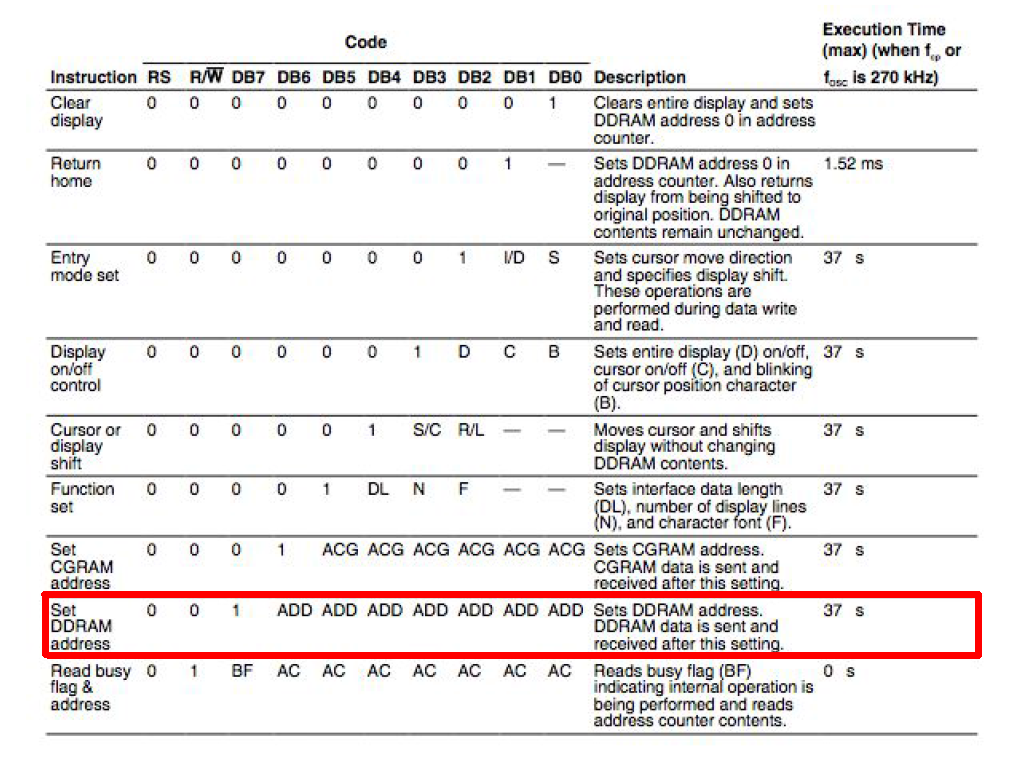
Each block in the LCD which displays a character is represented by a DDRAM block. Hence to set the cursor position we need to set the DDRAM address. This, we look up in the instruction sheet given above.
We need to set DB7 = 1 and DB6…DB0 to the address we want.
The addresses of 16x2 LCD are 0…15 for the first line and 64…79 for the second
line. 16 characters per line. So here is the required function:
void LCD_cursor_goto(int x, int y){
    char addr = 0x80; // Set DB7 to 1

    if(y==1)
        addr = addr + 0x40; // Start counting from 64(0x40) for line 2

    addr = addr + x; // Finally add x position to get address

    LCD_wait(); // wait until any previous command finishes

    LCD_command(addr); // Send command to LCD

}